


Please check the article "Last Updated" date above. I have been periodically updating this article with supplementary information. The main content is stable.
The ANAN-7000 can control the band switching of the ALS-1306 using its Open Collector (OC) Pins using a binary format. You can make your own data cable to connect the ANAN to the amplifier. It will be a 5 conductor cable with a DE-9 connectors.
For many popular name brand transceivers you can purchase interconnect cables already made. They can be costly and range from $30 to $90. The Yaesu interface sends binary ABCD data. The Kenwood interface uses serial RS232 data. The Icom interface uses voltage levels. The ANAN can perform band changing using ABCD binary over its OC Outputs.
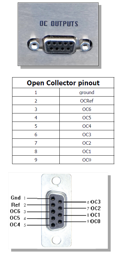
Above is the layout of the DE-9 connector on the ANAN-7000.
From the ALS-1306 schematic the following control information can be sent into the DE-9 connector on the rear of the amplifier marked RADIO INTERFACE. The control signal is binary. The logic level is TTL – 5v.
| Yaesu / Elecraft Band Change | |
| Band | DCBA |
| 60m | 0000 |
| 160m | 0001 |
| 80m | 0010 |
| 40m | 0011 |
| 30m | 0100 |
| 20m | 0101 |
| 17m | 0110 |
| 15m | 0111 |
| 10m | 1001 |
| 6m | 1010 |
| NC | 1111 |
The ANAN does not have an output dedicated for band control of an amplifier. However it does have 6 Open Collector (OC) outputs that can be programmed on a per-band basis. You can assign OC0, OC1, OC2 and OC3 to represent the ABCD binary signal to send to the ALS-1306. Open Collector means the output can pull a signal to ground (sink) when active but floats when inactive (no voltage coming from it.) The output devices are actually FETs rated at 25v 800ma. The band switch control voltage in the ALS-1306 is TTL, 5 volts and is well within the ANAN FET limits.
Since the ALS-1306 Band Switching input is 5+ TTL the ANAN will allow the amplifier’s input pins to float up to 5 volts and can pull them down to zero volts. This means the ANAN and the ALS-1306 can be directly connected between their DE-9 connectors.
For reference here is the ALS-1306 DE-9 pin definitions
|
ALS-1306 |
Function |
|
1 |
ABCD B In |
|
2 |
ABCD A In |
|
3 |
Kenwood Rx Data In |
|
4 |
Kenwood Tx Data Out |
|
5 |
Icom Band Data |
|
6 |
Ground * |
|
7 |
Amp Key In |
|
8 |
ABCD D In |
|
9 |
ABCD C In |
|
Shell |
Ground |
* If JP1 is not in place inside the amplifier the ground connection on Pin 6 is really a 10 ohm 1W resistor in parallel with two 2.7v back-to-back Zener diodes.
When Ground is not a Ground
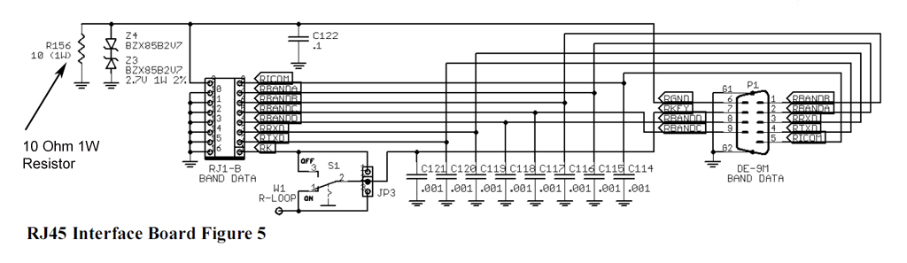
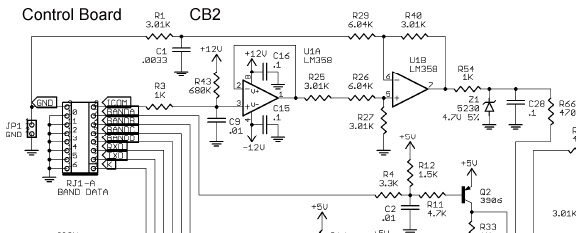
Here's the problem with the ground connection on pin 6 of the DE-9 connector on the amplifier. Pin 6 does not actually go to ground as the RGND label suggests. It goes to ground through a 10 ohm 1W resistor in parallel with two 2.7v back-to-back Zener diodes. Pin 9 on the RJ1-B connector goes to the Control Board CB2 pin 9 of RJ1-A. There is is called GND. But it's only really ground if JP1 is installed.
On my ALS-1306 JP1 was not installed as shipped.
Now consider this:
if
- you leave JP1 removed and
- you connect and use Pin 6 on the ALS-1306 DE-9 as your ground and
- you connect that to the ANAN ground on pin 1 of the ANAN DE-9
then
- you will essentially fully ground the amplifier Pin-6 anyway but through the interconnecting coax cable braid and the power cord ground wires!
endif
So here's the thing. If you want to use Pin 6 on the DE-9 as a ground you should install JP1 in the amplifier. You could also do as I did and use the DE-9 shell as the ground on the amplifier side of the cable. Since Ameritron never told me what JP1 and the 10 ohm resistor was for I decided not to use it and not to connect anything to it.
I just bothers me because 10 ohms is close to ground but it's not really ground. What are those 2.7v zener diodes for? Do they expect a +- 2.7v signal on this "ground" line? How does the amplifier respond to that?
Consulting with MFJ/Ameritron
According to Mark at Ameritron, JP1 is involved with the ICOM Band Control interface. The amplifier is shipped with JP1 removed. ICOM controls the band change using discrete voltage levels that are closely spaced. There is some kind of ground reference problem between the amplifier and some ICOM transceivers so they needed to raise the ground potential by a small amount. If you want a "real" ground on pin 6 of the DE-9 connector then install JP1. It probably will work fine without JP1 because of the common ground provided by the shield of the coax and any ground wires you attached to the amplifier and transceiver. If you installed JP1 and later desire to use an ICOM interface for band changing you may have to remove JP1.
Wiring the Interconnect Cable for the ANAN-7000
You need a DE-9 male connector for the ANAN end. If your a ANAN is an older model you will need a DB-25 male connector.
You need a DE-9 female connector for the ALS-1306 end.
You need a 5 conductor cable. It’s a good idea to use a shielded cable. I did not use one and have not experienced any problems. I will probably make a new one with a shielded cable in the future. Connect the shield to ground at only one end of the cable.
Wire your cable according to the following chart.
|
ALS-1306 Pins |
|
ANAN 7000 Pins |
||
|
Pin |
Signal |
|
Pin |
Signal |
|
6 |
Ground |
----- |
1* |
Ground |
|
2 |
A |
----- |
9 |
(OC-0) |
|
1 |
B |
----- |
8 |
(OC-1) |
|
9 |
C |
----- |
7 |
(OC-2) |
|
8 |
D |
----- |
6 |
(OC-3) |
* If you use a shielded cable connect the shield and the ground wire from the ANAN Pin 1 to the DE-9 shell at the ALS-1306 end. Alternatively you can install JP1 on Control Board CB2.
What is the purpose of the connection called OCRef on the Anan DE-9 Pin 2?
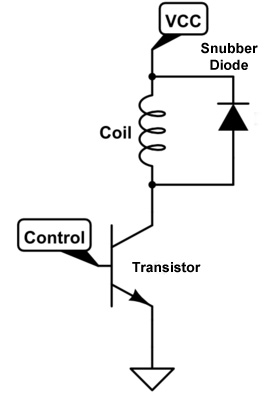 |
OCRef on the ANAN is only needed if you will be driving inductive loads (like relays) with the ANAN Open Collector outputs. Whenever you energize a coil and then de-energize it, the energy stored in the coil will try to be dumped back out of the coil in the opposite polarity of the original voltage. This voltage can be quite high and can damage a transistor that may have been driving the coil. It is customary to put a diode in parallel with the coil with the cathode on the power supply + side and the anode on the low side of the coil that goes to the driver transistor. The diode is called a snubber diode or flyback diode. It absorbs that back-EMF from the coil. In the case of the ANAN these diodes are already inside the transceiver. But the ANAN does not know what you will be connecting the transistors to and what the load voltage will be. If you were going to drive relays that had a 12v power supply then you would connect the OCRef pin to the +12v power at the other end. That would connect all of the cathodes of the ANAN diodes to +12v. That means that you can't mix the Open Collector outputs with relays that are not run from the same power supply. Since the ALS-1306 has a transistor buffer input with about a 4k input impedance and internally operating at +5v there is no need to worry about these diodes or protecting the open collector output driver on the ANAN. You can safely connect the ANAN Open Collector pins directly to the ALS-1306 ABCD pins. |
Programming Thetis OC Control
Next you will program the ABCD binary data into the Thetis OC Control screen. Keep in mind that the ANAN OC outputs are active low (negative logic). That means that we need to invert the ANAN signal to achieve the desired binary value.
|
Yaesu / Elecraft Band Change |
ANAN |
ANAN Thetis OC Programming ** |
||||
|
OC-1 |
OC-2 |
OC-3 |
OC-4 |
|||
|
Band |
DCBA |
DCBA |
A |
B |
C |
D |
|
160m |
0001 |
1110 |
|
X |
X |
X |
|
80m |
0010 |
1101 |
X |
|
X |
X |
|
60m * (off) |
1111 |
0000 |
||||
|
40m |
0011 |
1100 |
|
|
X |
X |
|
30m |
0100 |
1011 |
X |
X |
|
X |
|
20m |
0101 |
1010 |
|
X |
|
X |
|
17m |
0110 |
1001 |
X |
|
|
X |
|
15m |
0111 |
1000 |
|
|
|
X |
|
12m |
0001 |
1110 |
X |
X |
X |
|
|
10m |
1001 |
0110 |
|
X |
X |
|
|
6m |
1010 |
0101 |
X |
|
X |
|
|
NC |
1111 |
0000 |
|
|
|
|
* There is no band definition for 60m because there is a 200w power limit on that band.
The ALS-1306 does not have a 60m band position.
** These columns are the Inverted Binary value flipped horizontally with X = 1 and no check = 0
Electronic Signals OC-0 through OC-3 become Thetis values for OC-1 through OC-4 respectively
You program the OC Pins by band. Keep in mind that the Inverted DCBA signal is applied to OC Receive Pins 1-2-3-4 as ABCD. A binary 1 is a check and a binary 0 is no check. This can be REALLY CONFUSING. The wiring diagrams call the signals OC-0, OC-1, OC-2 and OC-3 but Thetis starts numbering them with 1. (No OC-0)
If you don’t want to rack your brain about this just wire the cable according to my chart and program Thetis according to the screen shot.
Here is a screen shot of the completed programming.
There are many ways to configure the radio programming which may require a different wiring order on the pins. Because of my digital and programming experience my thought process always has the least significant bit on the lowest signal ID. That means when I control the binary data with the OC pins I want to have the least significant bit (A) on OC-1 and the most significant bit (D) on OC-4. When you represent a binary number numerically on paper you show it with the least significant bit last as in DCBA. That's why I flip the DCBA horizontally to make it ABCD so that A lines up with OC-1, B lines up with OC-2, C lines up with OC-3 and D lines up with OC-4.
Another point or contention is using the term BCD (Binary Coded Decimal) to define the control signal. Technically this is not a BCD format signal. BCD is not the same as Hexadecimal. BCD is a way of counting in binary from 0 to 9. Nine in binary is 1001. The next binary number is 1010. BCD numbers stop at 9. You can see the bits to set the 6 meter band are binary 10 and that value is undefined in BCD. 1111 is also undefined in BCD. So even though Yeasu and Elecraft call this a BCD signal it really is not. It's a 4-bit binary control.

If you want you can use OC-5, 6 and 7 for control of other things per band as long as you leave OC-1, 2, 3 and 4 as they are.
Plug in the cable and set the amplifier band switch to REM for Remote. When you change the band on the ANAN the amplifier will follow and change to that band.
I believe this cable will work on the ALS-606 amplifier.
I believe this will work on older models such as the ANAN-200D by using a DB-25 connector instead of the DE-9 and wiring the DB-25 pins as follows.
|
ALS-1306 Pins |
|
ANAN 200D Pins |
||
|
Pin |
Signal |
|
Pin |
Signal |
|
6 |
Ground |
----- |
25 * |
Ground |
|
2 |
A |
----- |
5 |
(OC-0) |
|
1 |
B |
----- |
17 |
(OC-1) |
|
9 |
C |
----- |
4 |
(OC-2) |
|
8 |
D |
----- |
16 |
(OC-3) |
* If you use a shielded cable connect the shield and the ground wire from the ANAN pin 25 to the DE-9 shell at the ALS-1306 end. Alternatively you can install JP1 on Control Board CB2.
Good luck and happy band changing!